Taiwan Semiconductor Manufacturing Company (TSMC) has quietly emerged as Asia’s most valuable company by market cap. As at April 21st, 2026, the market value of TSMC was US$1.92 trillion based on its ADRs listed on NYSE. Only American companies, such as Nvidia, Google, Apple, Microsoft and Amazon, are bigger by market cap as shown below.
No.
Companies
US$ trillion
1
Nvidia
4.86
2
Google
4.00
3
Apple
3.91
4
Microsoft
3.15
5
Amazon
2.69
6
TSMC
1.92
7
Broadcom
1.90
TSMC has replaced Toyota Corporation of Japan as Asia’s most valuable manufacturing company, which was only US$260 billion (US$0.260 trillion). The closest Asia’s giant by market cap is Saudi Arabia’s national oil company, Aramco, at US$1.752 trillion.
The rise of TSMC
Many years ago, my Taiwanese friend, the late Dr Hsu of Hambrecht and Quist Asia Pacific based in Taipei, Taiwan, told me that his US colleague, Dr Morris Chang, was returning to Taiwan from the US to start TSMC at the Hsinchu Science Park, near Taipei. It would focus on contract manufacturing of ICs for IC design companies in Silicon Valley and Taiwan. Thus, these IC design companies would not need to establish their own foundries, which required substantial capital outlay. At that time, IC manufacturing was dominated by Intel. The IC design companies called fabless companies, often were started by Taiwanese engineers in Silicon Valley. One such company was Nvidia, which was started by Jensen Huang, a Taiwanese engineer in Silicon Valley.
Over the years, TSMC has emerged as very important company in the AI ecosystem, which helps Nvidia to design AI and manufacture them. In the process, TSMC has replaced Intel as the largest IC manufacturing company in the world, whose market cap was only US$0.33 trillion.
TSMCs’ manufacturing capability
TSMC operates its manufacturing facilities known as GIGAFAB fabs primarily in Taiwan, with major fabs in Hsinchu Science Park, Taipei, Southern Taiwan Science Park , Tainan, and Central Taiwan Science Park, Taichung. It is reported that TSMC has a production capacity of 15.02 million 12-inch equivalent wafer per year. It produces chips ranging from 2 microns to 3 nm. It has started mass production of 2 nm chip. This technology requires advanced manufacturing capability and features nanosheet transistors designed for superior energy efficiency and density, targeting AI and computing applications.
As at 2025, TSMC had about 90, 557 employeews. This is expected to increase as TSMC establishes new fabs in the US and Japan.
It has about 10,000 R&D staff, which is focusing on breakthroughs for 2 nm and beyond. At the same time, the R&D team is also focusing on FAB R&D to improve the fab process models like 2 nm. It is spending about US$6 billion in 2025, which was equivalent to 5% of revenue of US$120 billion.
TSMC is important to Taiwan, and it is a dominat driver of Taiwan’s economy. Its market value of US$1.92 trillion easily surpasses the GDP of Taiwan of about US$ 0.9 trillion.
My small investment in TSMC
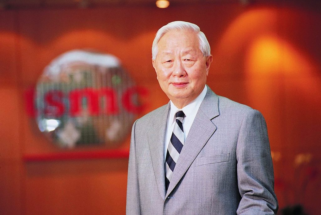
I have a small interest in TSMC through an investment in its ADRs via Moomoo trading platform. I am looking forward to TSMC achieving a market cap of US$2.0 trillion soon. I believe Taiwanese and the world would be thanking the late Dr Morris Chang for his vision of starting TSMC with the help of Taiwan’s government and Philips of Nederland. It was the pioneer of world’s dedicated “pure play” semiconductor foundry business model, solely focusing on manufacturing IC chips for other companies. It also helped fabless IC design companies to develop various chip for many applications. It is truly Asia’s global manufacturing giant located in a tiny country of Taiwan.
Charles Goodyear received US patent for vulcanized natural rubber
Charles Goodyear was an American inventor who revolutionized the rubber industry with his discovery of vulcanization. Before his breakthrough, natural rubber was prone to becoming sticky and brittle in hot or cold weather, making it impractical for many industrial applications. Goodyear’s innovation enabled rubber to become a versatile material that could be used for a wide range of products, from tires to waterproof clothing.
Born in New Haven, Connecticut in 1800, Goodyear struggled financially throughout his life, often facing bankruptcy and financial ruin. Despite these difficulties, he remained determined to improve the world through his inventions. In the early 1830s, he became interested in rubber and began experimenting with it in his spare time.
Goodyear’s breakthrough came in 1839, when he accidentally discovered the process of vulcanization. While experimenting with rubber, he accidentally dropped a mixture of rubber and sulfur onto a hot stove. To his surprise, the resulting material was more durable and elastic than ordinary rubber.
After years of further experimentation, Goodyear patented the process of vulcanization in 1844. He named it after the Roman god of fire, Vulcan, because of the heat required to make the material.
Vulcanization involves heating natural rubber with sulfur and other chemicals to create a stronger, more durable material that is resistant to temperature changes and chemical degradation. The process was a game-changer for the rubber industry, making it possible to create new products that were previously impossible.
Goodyear’s invention helped to create a new industry in the United States, leading to the growth of companies such as Goodyear Tire and Rubber Company, which is still a major manufacturer of tires today. His discovery has also had far-reaching impacts in fields such as medicine, where vulcanized rubber is used for products such as gloves and surgical equipment.
Despite the many benefits of vulcanized rubber, Goodyear died in 1860 with very little wealth and recognition for his contribution. Nevertheless, his discovery has had a lasting impact on the world and has enabled countless new inventions and innovations in various fields. Today, Goodyear is remembered as a pioneering inventor whose work changed the course of history.
Immense contribution to Malaysia
Women tapping rubber trees to collect rubber latex
The invention of vulcanized natural rubber contributed to the development of the natural rubber industries, especially rubber tyres for the car industry in the late 9th century and the early 20th century. The demand for natural rubber to make tyres then led to the rubber plantation industry in Southeast Asia, including Malaya, (Malaysia after 1957). Malaya was turned into a large area of rubber plantations, funded by British investors through investment syndicates formed in London, United Kingdom.
We, Malaysians, owed our gratitude to Charles Goodyear.
Rubber tree: An important economic tree in British Malaya
British Malaya (then Malaysia) used to be the major producer of natural rubber, gutta percha and tin. These three commodities made British Malaya an important British colony in the late 19th century and the early 20th century.
Natural rubber industry is no longer important in Malaysia, as rubber has been replaced by oil palm as the most important industrial crop in the country since the 1970s. However the economic and social impacts of the natural rubber industry have been very significant for Malaysians during the period from late 19th century to 1970s.
In the next few articles, we will be covering various aspects of the natural rubber industry, from its development in British Malaya, the innovators of the rubber products and the decline of the rubber industry. Every pupil in Malaysia knew that the seeds of rubber trees originally were smuggled out of Brazil. Later they came to British Malaya.
The first of the article is how I membered about rubber trees and daily activities revolving around rubber.
Rubber trees and daily tapping of latex
An early clone of rubber tree used to be able to be productive after 5 to 7 years. The bark needs to be tapped to allow the bark to “bleed” a white latex. The white latex is collected in a cup made of porcelain. The work of a rubber tapper started early in the morning at about 6 am. My parents used to have a small holding of rubber trees about a few kilometres from our home in Beranang, Selangor, Malaysia, in the 1960s. They cycled to the rubber small holding about 6.00 am, with a sharp rubber tapping knife. First, using a headlight light for illumination, they removed a thin slice of the rubber bark which was enough for the rubber latex to “bleed” and to be collected in the attached cup. They would take about an hour to complete the tapping of rubber trees in the small holding. By 8.00 am, the cups would be filled with white rubber latex. Then, they emptied the cups containing rubber latex to a big pail.
The pails would be placed onto the bicycle and transported to a communal rubber rolling centre. Every village would have a communal rolling centre to process the rubber latex into rubber sheets.
At the communal rolling centre, a measured amount of formic acid would be added to the rubber latex which had been poured into a special rectangular steel container. After a while, the rubber latex would coagulate, separating water from rubber. The rubber was still soft and about 4 to 5 cm thick. The soft block of rubber would be passed through an iron roller to reduce the thickness of rubber block to about 1 cm. The remaining water in the rubber block would have been completely removed after going through several times of rolling. Finally, the thin rubber sheet was dried in the sun to remove the remaining water. The dried drubber sheet would turn slightly brown after several days under the sun. The rubber was now ready to be sold for cash.
Rolling rubber sheet to remove water
The tapping of rubber trees and the conversion of rubber latex into rubber sheets would take from 6 am to about 12.00 noon, every day.
After resting for lunch, most villagers would go to the their small paddy field to prepare their rice fields or to harvest their paddy. The rice filed would become their supplementary income after rubber sheets. In every town in Malaysia, there would be rubber dealers who would buy the rubber sheets at “discounted prices” after quality checks.
As expected, rubber small holders and the villagers were poor, surviving from selling of rubber sheets. This was compounded by the fluctuations of prices of rubber sheets on the world market. At time of high rubber prices, they would purchase a new bicycle for the family or a having “a feast” with the first-harvest of rice from the paddy field.
Rubber plantation companies were wealthy
The rubber small holding sector was a not a significant segment of the rubber industry. Rubber estates or plantations were much bigger with substantial acreage. The rubber estates boomed in the early 1900s to 1930’s when the motor industry emerged in Europe, US and Japan, thanks to Mr Henry Ford. In the early 1900s investment syndicates based in London drew investors, both individuals and institutions, to invest in rubber estates in British Malaya. At the time, British administrators in British Malaya opened up a vast area of forest to be cleared to plant rubber. Established British companies in British Malaya also attracted investors to buy smaller rubber estates to be consolidated into larger estates.
If we were to travel by car in British Malaya in the 1930s, rubber estates with British names would be scattered throughout British Malaya. These rubber estates would be managed by British planters, with the help of locals. They employ mostly Indian rubber tappers brought in from India, who were paid low salaries.
The larger rubber estates would have their own golf courses and social clubs. My wife’s late mother described the lives of the British planters vividly. She was about ten and lived in Rantau, Negeri Sembilan, Malaysia, where her village was surrounded by one of largest rubber estates in British Malaya.
“ Every evening, about 6 pm, I saw many cars, driven by Malay drivers, cruising to the Club in the centre of the town. The “missuses” of the British planters wore nice dresses, which were different from those worn by the local women.”
There was the days when rubber was the economic pillar of the economy of British Malaya.
Everyone knew that the rubber sheets sold to local rubber dealers would be destined to Europe. Very few would know that the innovations that led to the use of natural rubber into industrial products, notably tyres, were created much earlier in the mid of the 19th century. Many of these innovators went bankrupt many times during the innovative pursuits.
The next article would cover these innovators, which had transformed British Malaya from a nation of mainly forests to a modern economy driven by rubber trees. As Malaysians now, we should salute these innovators, such as the Hancocks of Marlborough and Charles Goodyear.
Five LED pioneers, comprising Isamu Akasaki, Shuji Nakamura, Nick Holanyak Jr, M. George Craford and Russel Dupuis, were awarded the 2021 Queen Elizabeth Prize for Engineering. They joined a list of distinguished individuals for their contribution to the engineering world and humanity. The five LED pioneers shared a prize of £1.0 million.
The Queen Elizabeth Prize for Engineering, also known as the QEPrize, is a global prize for engineering and innovation. The prize was launched in 2012. It is run by the Queen Elizabeth Prize for Engineering Foundation, which is a charitable company. The QEPrize receives donations from, large International companies.
The Queen Elizabeth Prize for Engineering is awarded for engineering-led advances that are judged to be of tangible and widespread benefit to the public. The foundation invites nominations from the public, engineering and science academies, universities, research organizations, and commercial organizations from anywhere in the world.
The judging panel works from the information provided in the nomination, comments from referees and any other information required in order to establish which nomination most fully meets the following prize criteria.
What s it that his person has done ( or up to five people have done) that is ground-breaking innovation in engineering?
In what way has this innovation been of global benefit to humanity?
Is there anyone else who might claim to have had a pivotal role in this development?
The winner (winners) of the QEPrize are announced every two years by the chairman of the QEPrize Foundation. To-date, nineteen individuals have been awarded the QEPrize, namely from US, Japan, France and UK.
(1), (2), and (3): Robert Kahn, Vinton Cerf and Louis Puzin for their contribution to the protocols that make up the fundamental architecture of the internet.
(4): Tim Berners-Lee for his contribution as the creator of the World Wide Web.
(5): Marc Andreessen for his contrition as the creator of the Mosaic web browser.
(6): Robert Langer for work in controlled-release large molecule drug delivery.
(7): George E. Smith for the invention of the charge-coupled device (CCD) principle.
(8): Michael Tompsett for the development of the CCD image sensor, including the invention of the imaging semiconductor circuit and the analogue-digital converter.
(9): Nobukazu Teranishi for the creation of the pinned photodiode (PPD).
(10): Eric Fossum for developing the CMOS image sensor.
(11): Bradford Parkinson for leading the development, design, and testing of key GPS components.
(12): James Spilker, Jr for developing the L-band GPS civil signal structure using CDMA.
(13): Hugo FrueHauf for his role in creating a highly accurate miniaturized atomic clock using a rubidium oscillator.
(14): Ricard Schwartz for leading the design and development of the highly robust, long-lasting Block I satellites.
(15): Nick Holonyak for developing the first (red) visible-light light emitting diode.
(16): Isamu Akasaki for the development of blue and white LED.
(17): M. George Crayford for developing the yellow LED and pioneering the development of AllnGaP LEDS using metal organic chemical vapor deposition (MOCVD).
(18): Shuji Nakamura for the development of blue and white LEDs
(19): Russel Dupuis for demonstrating that MOCVD could be applied to high-quality semiconductor thin films and devices to produce high performance LEDs.
We hope the QEPrize and Nobel prize would spur young scientists and engineers to develop innovations for humanity. We also hope that Malaysian scientists and engineers would be among the recipients of these QEPrize and Nobel prizes.
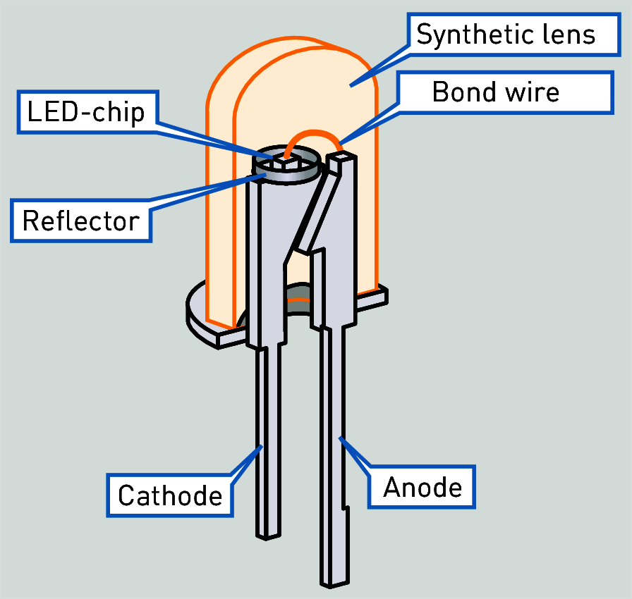
An LED, which stands for light-emitting diode, is a semiconductor diode that glows when a voltage is applied. Devices with LEDS are everywhere in our house: televisions, mobile phones, solar flood lights, torchlights, inhouse lighting, street lightings, and cars day- indicator lights. .
Many companies are producing LED lights, and there are ample choices to buy indoor lights, which previously were made by Philips and Osram using the older fluorescent lights. .
The working of an LED
In my MIT Sloan days, a well-known Professor of Innovation, James M. Utterback, brought to the class a collection of hairs (animal and human) that were used by Thomas Edison to develop his filament bulbs. Since then, filament bulbs have been used to light homes. Sadly, these filament bulbs would be largely substituted by LED lights of various shapes and sizes.
The workings of the LED bulb are vastly different from that of the older incandescent lightbulb. The incandescent light bulb works by running electricity through a filament that is inside the glass bulb. The filament heats up and glows, and that creates the light. However, it also creates a lot of heat. The incandescent light bulb loses about 98% of its energy-producing heat, making it quite inefficient.0datret light.
LED was built from a series of inventions
LEDs are part of a new family of lighting technologies called solid-state lighting; LEDs are cool to the touch. Instead of one lightbulb, in an LED lamp there are many small light-emitting diodes.
LEDs create light by electroluminescence in a semiconductor material. Electroluminance is a phenomenon of a material emitting light when electric current or an electric field is passed through it. This happens when electrons are sent through the materiel and fill electron holes. An electron hole exists where an atom lacks electrons (negatively charged) and therefore has a positive charge. Semiconductor materials like germanium or silicon can be “doped” to create and control the number of electron holes. Doping is the adding of other elements to the semiconductor material to change its properties. By doping a semiconductor, we can make two separate types of semiconductors in the same crystal. The boundary between the two types is called a p-n junction. The junction only allows current to pass through it one way. This is why they are used as diodes. LEDs are made using p-n junctions, As electrons pass through one crystal to the other they fill electron holes. They emit photons (light). This a complex process.
The pioneers of the LED
Currently the LED light is popular due to its efficiency and many believe it is a “new technology”. The LED, as we know it, has been around for over 50 years. The recent development of white LED is what has brought it into the public attention as a replacement for other white light sources.
The current state of the development of the LED was built on a series of innovations and their innovators. Many innovators have helped create the LED lights that are used today.
These innovators include:
Henry Joseph Round
Electro luminesce, the natural phenomenon upon which LED technology is built, was discovered in 1907 by a British radio research and assistant to Guglielmo Marconi, Henry Joseph Round, while experimenting with silicon carbide and a cat’s whisker.
Oleg Vladimirovich
During the 1920s, Russian radio researcher Oleg Vladimirovich was studying the phenomena of electroluminescence in diodes in radio sets. In 1927, he published a paper “Luminous Carborundum (silicon carbide) Detector and Detection with Crystals” detailing his research. While no practical LED was created at that time based on his work, his research did influence future inventors
Robert Biard and Gary Pittman
Years later in 1961, Robert Biard and Gary Pittman invented and patented an infrared LED for Texas Instruments. This was the first LED. However, since it was infrared, it was beyond the visible light spectrum. Human cannot see infrared light. Biard only accidentally invented a light-emitting diode while they were actually attempting to invent a laser diode.
Nick Holonyack
In 1962, Nick Holonyack, a consulting engineer for General Electric, invented the first visible light LED. It was a red LED and Holonyack used gallium arsenide phosphide as a substrate for the diode. Holonyack has earned the honour of being called the “Father of light -emitting diode” for his contribution. .
He also holds 41 patents and his other inventions include the laser diode and the first light dimmer.
M. George Craford
In 1972, electrical engineer, M. George Craford, invented the first yellow-coloured LED for Monsanto using gallium arsenide phosphide in the diode. Craford also invented a red LED that was 10 times brighter than Holonyack’s.
Monsanto was the first company to mass-produce visible LEDs. In 1968. Monsanto produced red LEDs used as indicators. But it was not until the 1970s that LED became popular when n Fairchild Optoelectronics began producing low-cost LED devices for manufacturers.
Herbert Maruska and Waalden C. Rhines.
In 1986, Herbert Maruska and Walden C. Rhines from Stanford University, US, created a working blue LED using magnesium, and set all future standards.
Isamu Araski and Hiroshi Amano
In 1993, physicists Isamu Araski and Hiroshi Amano developed a high-quality gallium nitride for blue LEDs.
Shuji Nakamura
In 1979, Shuji Nakamura developed the world’s first bright blue LED using gallium nitride. It wouldn’t until the 1990s that the blue LED would become low cost for commercial production. These developments led to the development of white LEDs.
The Importance of white light LEDs
Blue LEDs have been developed based on gallium nitride and silicon carbide materials. Production of light in this shorter-wavelength, more energetic region of the visible spectrum, has long been elusive to designers of LEDs. High photon energies (light) typically increase the failure rate of semiconductor devices, and the low sensitivity of the human eye to blue light adds to the brightness requirement for a useful blue diode. One of the most important aspects of a blue LED is that it completes the red, green, and blue (RGB) primary color family to provide an additional mechanism of producing solid-state white light, through the mixing of these component colors.
The addition of bright blue-emitting LED to the earlier-developed red and green devices makes it possible to use three LEDs, tuned up to an appropriate output levels, to produce any color of the visible light spectrum, including white. Other possible approaches to producing white light, utilizing a single device, are based on phosphor or dye wavelength converters or semiconductor wavelength converters. The concept of white LED is particularly attractive for general illumination, due to the reliability of solid-state devices, and the potential for delivering very high luminous efficiency as compared to conventional incandescent and fluorescent sources.
The human eye perceives light as being white if the three types of photosensory cone cells, located in the retina, are attenuated in particular ratios. The three cone types exhibit response curves that peak in sensitivity at wavelength representing red, green and blue, and the combination of these response signals produces various color sensations in the brain. A wide variety of different color mixtures are capable of producing a similar perceived color, especially in the case of white, which may be realized through many combinations of two or more colors.
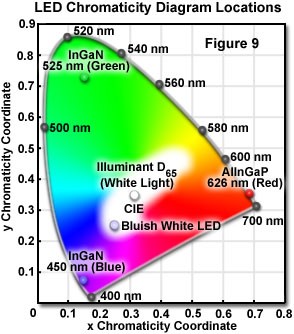
A chromaticity diagram is a graphical means of representing the results obtained from mixing colors. Monochromatic color appear on the periphery of the diagram, and a range of mixture representing white is located in the central region of the diagram. Light that is perceived as white can be generated by different mechanisms. A chromaticity diagram is shown in Table 1.
Table 1: LED chromaticity diagram
One method is to combine light of two complementary colors in the proper power ratio. The ratio that produces tristimulus response to the retina (causing perception of white) varies for different color combinations.
A selection of complementary wavelengths, along with the power ratio for each pair that produces the chromaticity coordinates of a standard illuminant is designated D(65) by the International Commission for Illumination (CIE, Commission Internationale de I’Eclairage).
Another means of generating white light is by combining the emission of three colors that will produce the perception of white light when they are combined in the proper power ratio. White light can also be produced by broadband emission from a substance that emits over a large region of the visible spectrum. This type of emission approximates sunlight, and is perceived as white. Additionally, broadband emission can be combined with emission at discrete spectral line to produce a perceived white, which may have particular desirable color characteristics that differ from these of white light produced by other techniques.
The combination of red, green, and blue diode chips into one discrete package, or in a lamp assembly housing a cluster of diodes, allows the generation of white light or any of 256 colors by utilizing circuitry that drives the three diodes independently. In applications requiring a full spectrum of colors from a single point source, this type of RGB diode format is the preferred technique.
Most white-light diodes employ a semiconductor chip emitting at a short wavelength (blue, violet or ultraviolet) and a wavelength converter, which absorbs light from the diode and undergoes secondary emission at a longer wavelength. Such diodes, therefore, emit light of two or more wavelengths, that when combined, appear as white. The quality and spectral characteristics of the combined emission vary with the different design variations that are possible. The most common wavelength converter materials are termed phosphors, which exhibit luminescence when they absorb energy from another radiation source. The typically utilized phosphors are composed of an inorganic host substance containing an optically active dopant. Yttrium aluminium garnet (YAG) is a common host material, and for diode applications, it is usually doped with one of the rare-earth elements or a rare-earth compound. Cerium is a common dopant element in YAG phosphors designed for white light emitting diodes.
The first commercially available white LED (fabricated and distributed by the Nichia Corporation) was based on a blue-light-emitting gallium-indium-nitride (GaInN) semiconductor device surrounded by a yellow phosphor. The phosphor is Ce-doped YAG, produced in powder form and suspended in the epoxy resin used to encapsulate the die. The phosphor-epoxy mixture fills the reflector cup that supports the die on the lead frame, and a portion of the blue emission from the chip is absorbed by the phosphor and reemitted at the longer phosphorescence wavelength. The combination of the yellow photo-excitation under blue illumination is ideal in that only one converter species is required. Complementary blue and yellow wavelengths combine through additive mixing to produce the desired white light. The resulting emission spectrum of the LED represents the combination of phosphor emission, with the blue emission that passes through the phosphor coating unabsorbed.
The relative contributions of the two emission bands can be modified to optimize the luminous efficiency of the LED, and the color characteristics of the total emission. These adjustments can be accomplished by changing the thickness of the phosphor-containing epoxy surrounding the die, or by varying the concentration of the phosphor suspended in the epoxy. The bluish white emission from the diode is synthesized, in effect, by additive color mixing, and its chromaticity characteristics are represented by a central location (0.25, 0.25) on the CIE chromaticity diagram ( Bluish White LED).
White light diodes can generate emission by another mechanism, utilizing broad-spectrum phosphors that are optically excited by ultraviolet radiation. In such devices, an ultraviolet-emitting diode is employed to transfer energy to the phosphor, and the entire visible emission is generated by the phosphor. Phosphors that emit at a broad range of wavelengths, producing white light, are readily available as the materials used in fluorescent light and cathode ray tube manufacture. Although fluorescent tubes derive their ultraviolet emission from a gas discharge process, the phosphor emission stage producing white light output is the same as in ultraviolet-pumped white diodes. The phosphors have well known color characteristics and diodes of this type have the advantage that they can be designed for applications requiring critical color rendering. A significant disadvantage of the ultraviolet-pumped diodes, however, is their lower luminous efficiency when compared to white diodes employing blue light for phosphor excitation. This results from the relatively high energy loss in the down-conversion of ultraviolet light to longer visible wavelengths.
Dyes are another suitable type of wavelength converter for white diode applications, and can be incorporated into the epoxy encapsulant or in transparent polymers. The commercially available dyes are generally organic compounds, which are chosen for a specific LED design by consideration of their absorption and emission spectra. The light generated by the diode must match the absorption profile of the converting dye, which in turn emits light at the desired longer wavelength. The quantum efficiencies of dyes can be near 100 percent, as in phosphor conversion, but they have the disadvantage of poorer long-term operational stability than phosphors. This is a serious drawback, as the molecular instability of the dyes causes them to lose optical activity after a finite number of absorptive transitions, and the resulting change in light emitting diode color will limit its lifetime.
White light LEDs based on semiconductor wavelength converters have been demonstrated that are similar in principle to the phosphor conversion types, but which employ a second semiconductor material that emits a different wavelength in response to the emission from the primary source wafer. These devices have been referred to as photon recycling semiconductors (or PRS-LEDs), and incorporate a blue-emitting LED die bonded to another die that responds to the blue light by emitting light of a complementary wavelength. The two wavelengths then combine to produce white. One possible structure for this type of device utilizes a GaInN diode as a current-injected active region coupled to an AlGaInP optically-excited active region. The blue light emitted by the primary source is partially absorbed by the secondary active region, and “recycled” as reemitted photons of lower energy. In order for the combined emission to produce white light, the intensity ratio of the two sources must have a specific value that can be calculated for the particular dichromatic components. The choice of materials and the thickness of the various layers in the structure can be modified to vary the color of the device output.
Because white light can be created by several different mechanisms, utilizing white LEDs in a particular application requires consideration of the suitability of the method employed to generate the light. Although the perceived color of light emitted by various techniques may be similar, its effect on color rendering, or the result of filtration of the light, for example, may be entirely different. White light created through broadband emission, through mixing of two complementary colors in a dichromatic source, or by mixing of three colors in a trichromatic source, can be located at different coordinates on the chromaticity diagram and have different color temperatures with respect to illuminants designated as standards by the CIE. It is important to realize, however, that even if different illuminants have identical chromaticity coordinates, they may still have substantially different color rendering properties, due to variations in details of each source’s output spectrum.
Two factors, referred to previously, are of primary importance in evaluating white light generated by LEDs: the luminous efficiency, and the color rendering capabilities. A property referred to as the color rendering index (CRI) is utilized in photometry to compare light sources, and is defined as the source’s color rendering ability with respect to that of a standard reference illumination source. It can be demonstrated that there exists a fundamental trade-off between luminous efficiency and color rendering ability of light-emitting devices. For an application such as signage, which utilize blocks of monochromatic light, the luminous efficiency is of primary importance, while the color rendering index is irrelevant. For general illumination, both factors must be optimized.
The spectral nature of the illumination emitted from a device has a profound influence on its color rendering ability. Although the highest possible luminous efficiency can be obtained by mixing two monochromatic complementary colors, such a dichromatic light source has a low color rendering index. In a practical sense, it is logical that if a red object is illuminated with a diode emitting white light created by combining only blue and yellow light, then the appearance of the red object will not be very pleasing. The same diode would be quite suitable for backlighting a clear or white panel, however. A broad-spectrum white light source that simulates the sun’s visible spectrum possesses the highest color rendering index, but does not have the luminous efficiency of a dichromatic emitter.
Phosphor-based LEDs, which either combine blue emission wavelengths with a longer-wavelength phosphorescence color, or create light solely from phosphor emission (as in ultraviolet-pumped LEDs), can be designed to have color rendering capabilities that are quite high. They have color character that is similar in many respects to that of fluorescent lamp tubes. The GaInN LEDs utilize blue emission from the semiconductor to excite phosphors, and are available in cool white, pale white, and incandescent white versions that incorporate different amounts of phosphor surrounding the chip. The cool white is the brightest, utilizing the least phosphor, and produces light with the most bluish color. The incandescent white version surrounds the blue-emitting chip with the most phosphor, has the dimmest output, and the yellowest (warmest) color. The pale white has brightness and color shade characteristics intermediate between the other two versions.
The availability of white LEDs has generated great interest in applying these devices to general lighting requirements. As lighting designers become familiar with the characteristics of the new devices, a number of misconceptions will have to be dispelled. One of these is that the light from a white LED can be used to illuminate a lens or filter of any color, and maintain the accuracy and saturation of the color.
In a number of the versions of white LED, there is no red component present in the white output, or there are other discontinuities in the spectrum. These LEDs cannot be used as general sources to backlight multicolored display panels or colored lenses, although they function well behind clear or white panels. If a blue-based GaInN white LED is employed behind a red lens, the light transmitted will be pink in color. Similarly, an orange lens or filter will appear yellow when illuminated with the same LED. Although the potential benefits in application of LEDs are tremendous, consideration of their unique characteristics is necessary in incorporating these devices into lighting schemes in place of more familiar conventional sources.
Conclusion
White LEDs are becoming popular sources of while lights. There were many inventors involved since the early 1900s to bring about this useful and practical white LEDs and its applications.
Let us salute those inventors who were from various nationalities.
Aspirin is an effective and inexpensive medicine that millions take daily to prevent heart attacks and strokes. Who could improve on that?
The inventor of aspirin
In ancient times, salicylate-containing plants such as willow were commonly used to relieve pain and fever. A salicylate is a salt or ester of salicylic acid . Salicylates are thought to protect the plant against insect damage and disease. Aspirin is a derivative of salicylic acid. It is known as acetylsalicylic acid.
In 1897, a German chemist, Dr. Felix Hoffman, working for the Bayer company, was able to modify salicylic acid to create acetylsalicylic acid, which was named aspirin. However, the company dismissed the market potential of aspirin on the ground that it had an “enfeebling” action on the heart. At that time, the company was more interested on the potential of another new drug-heroin, which was also synthesized by the company.
Subsequently, aspirin was found to be more tolerable to the stomach than salicylic acid, which led to the widespread use of aspirin for pain relief. Furthermore, Hoffman’s acetylation of salicylic acid also proved its ability to prevent cardiovascular events. Aspirin, was considered by many as a wonder drug.
One common adverse effect of aspirin is an upset stomach. More significant side effects include stomach ulcers, stomach bleeding and worsening asthma. Aspirin is not recommended in the last part of pregnancy.
Aspirin is one of the most widely used medications globally, with an estimated 40,000 MT (50 to 120 billion pills) consumed each year. It is on the World Health Organization’s List of Essential Medicines. It is available as a generic medication. In 2018, it was the 40th most commonly prescribed medication in the US, with more than 19 million prescriptions (wikepedia).
According to Bayer, the history of aspirin can be summarized in the following milestones.
1897
In a Bayer laboratory in Wuppertal, Germany, Dr Felix Hoffman was the first to succeed in synthesizing a chemically pure and stable form of acetylsalicylic acid (ASA), which became the active ingredient of aspirin.
1899
Aspirin was registered as a trademark. It was launched on the market in powder form. Bayer delivered the medicine to pharmacies in small 250-grams glass vials. 500 mg of the powder was then weighed out and dispensed to customers in small paper bags. One year later, Bayer launched the analgesic in the classic tablet form-one of the first medicines to be marketed in dosage form.
1915
Aspirin became available without prescription and became a best-seller in the US.
1949
Aspirin turned 50, and the following year, was the first time it featured in the Guinness Book of Records as the most frequently sold pain reliever in the world.
1969
A box of aspirin flied to the moon aboard Apollo 11.
1977
A study reported that aspirin could prevent ischemic stroke in appropriate patients. In the same year, the World Health Organization introduced its “Essential Drug List. Aspirin was included right from the start as an essential analgesic.
1997
Acetylsalicylic acid, the active ingredient in aspirin, celebrated its centenary.
1999
Aspirin took its place among such medical advances as the stethoscope and artificial heart when it was inducted into the Smithsonian Institution’s Museum of American History, US.
2004
British researcher Professor Derek W. Gilroy elucidated the anti-inflammatory properties of aspirin.
2012
Publication in the journal Headache by Lampl et al, which reaffirmed the effectiveness of aspirin as a first-time treatment of migraine or episodic tension type headache and found that pre-treatment headache did not predict potential success or failure of aspirin.
2014
The active ingredient of new aspirin, acetylsalicylic acid, was used in the form of microparticles that were on average 10 per cent of size of particles found in previous aspirin tablets.
Microparticles were combined with sodium carbonate, which acted as a disintegrant and local buffer, helping new aspirin dissolved more quickly, entered the bloodstream faster, and relieved pain twice as fast as previous aspirin tablets.
(Source: bayer.com/en/products/aspirin)
Enter a “new aspirin”: Vazalore
A US-based company, PLx Pharma (www.plxpharma.com) is trying to do that. According to the Barron’s online on September 20th, 2021, there has been no innovation in the aspirin market in over 50 years. The company, based in Sparta, New Jersey, US, is seeing an opportunity to launch a new product, Vazalore, in some 30,000 retail drug stores in the US.
The aspirin market is a crowded field, where aspirin has been around since 1899. The company noted that Vazalore’s advantage is that it reduces aspirin’s tendency to irritate the stomach for people who use it regularly, a problem that can lead to ulcers. In addition, Vazalore has been shown to achieve better absorption than coated aspirin, according to studies by Harvard Medical School cardiologist Deepak Bhatt, who heads PLx Pharma scientific advisory board. PLx Pharma is facing the challenge of convincing existing users of aspirin to switch to Vazalore. Vazalore will cost US$25 a month versus a few dollars for coated aspirin. It is estimated that 43 million Americans take aspirin on their doctor’s advice, plus millions more to treat the symptoms of arthritis and other ailments. The company estimates that every new customer will be worth US$230 a year to PLx Pharma, so that it could realize US$100 million in annual revenue from each 1 pe cent of those 43 million people.
The Vazalore capsule holds a liquid formulation of aspirin bound up in lipid, which prevents the aspirin’s release until it passes through the stomach to the intestine. It was reported that PLx Pharma will apply its patented technology to ibuprofen and other drugs that give some users stomach problems.
We doubt users of aspirin will drop it anytime soon.
The rapid Covid-19 vaccination drive in Malaysia has highlighted that there are a big group of Malaysians who have fear of needles being injected into their arms. Many would be recipients of vaccines missed their appointments. Others have high blood pressure before receiving their vaccines. One of these needle-phobics is my wife. Fortunately, she had received both Covid-19 jabs after a doctor gave her a medication to calm her down before her injection.
Now there is good news for these needle-phobics. An article in the London Guardian on August 2nd, 2021, reported that people would be able to be vaccinated without using the dreaded needles.
The sight of a needle piercing skin is enough to put a fear on a quarter of adult Britons and trigger up to 4% into fainting. But hope is on the horizon for needle-phobics as researchers are working on a range of non-injectable Covid vaccine formulations, including nasal sprays and tablets.
Almost every vaccine in use today comes with a needle, and the approved Covid-19 vaccines are no exception. Once jabbed, the body’s immune system usually mounts a response, but scientists in the UK and beyond are hoping to harness the immune arsenal of the mucous membranes that line the nose, mouth, lungs and digestive tract, regions typically colonised by respiratory viruses including Covid-19, in part to allay the fears of needle-phobics.
To understand the role this anxiety may be playing in vaccine hesitancy in the UK and other parts of the world, Daniel Freeman, a professor of clinical psychology at the University of Oxford, and colleagues recruited more than 15,000 adults – representative of age, gender, ethnicity, income and region of the UK population – in a study and found that a quarter of the group screened positive for a potential injection phobia.
Notably, this subset of people were twice as likely to report that they would put off getting vaccinated or indeed never get the jab. Out of the total number of those fearful of needles, 10% were found to be strongly Covid vaccine-hesitant.
Probably about 3% to 4% of the UK’s total adult population were needle-phobic (have an intense fear of medical procedures involving injections), he said. And the fear of needles was more prevalent in younger adults, he added. “So, potentially, needle phobia explains more of the hesitancy in younger people.”
“The fear of needles is the one type of anxiety where actually you can faint and that sort of fear and sometimes the embarrassment about fainting is a powerful driver that people want to avoid.”
This avoidance, among other reasons, has spawned efforts to develop Covid-19 vaccines in the form of inhaled vapours, tablets, oral drops or intranasal sprays.
Dr Stephen Griffin, a virologist at Leeds University, said he was constantly asked by UK healthcare staff when there would be non-injectable formulations of Covid vaccines – not just for patients, “but because there are so many needle-phobic staff”.
Non-injectable vaccines could be gamechangers for many other reasons. Room-temperature formulations could be a boon for countries that don’t have the logistical resources to handle the ultra-cold requirements of existing Covid vaccines. Crucially, targeting mucosal tissues has the potential to produce “sterilising immunity”, or the complete elimination of infection in the body, thereby theoretically thwarting transmission. Current intramuscular vaccines, though dramatically effective in preventing serious illness and death, cannot stop transmission altogether.
But there have been hiccups in the quest for non-injectable vaccines – for instance, an existing nasal spray flu vaccine has been shown to outperform flu shots in young children, but its performance is muted in adults. And in June, the US biotech company Altimmune abandoned its intranasal Covid vaccine project, saying that it generated weaker than expected immune responses in an early trial.
At the moment, there are many researchers in the early stages of developing a non-injectable Covid vaccine. An Oxford/AstraZeneca aerosolised formulation is in development, and the Chinese biotech company CanSino Biologics recently kicked off the development of its inhaled vaccine. Others looking at nasal sprays include a team at Lancaster University, which is expected to report data from animal trials imminently, as well as the US-based Cadogenix and India’s Bharat Biotech. Drugmakers are also looking at oral alternatives, such as the San Francisco-based Vaxart, which has completed an early human study on its tablet.
My wife told me that many of her friends have refused to be vaccinated for Covid-19 due to their fear of needles and other many reasons. Hopefully, they will protect themselves and others from Covid-19 infections if needleless vaccination is available.
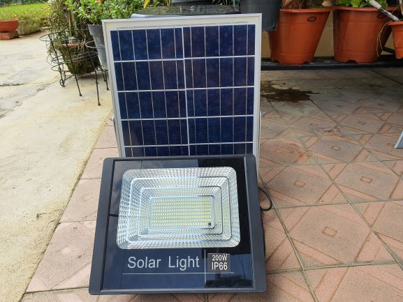
Every day I use solar flood lights to deter wild monkeys from feasting on my ripe rambutans. Hopefully, the flood lights will also deter unwanted strangers from stealing the ripe rambutans. I recharge the solar flood lights using solar panels.
Many are interested to know who invented the solar panels that let us to harvest the sunlight and to be stored in the batteries of the solar flood lights. I purchase the solar flood light from an ecommerce platform at about US$50 a unit.
Solar panels have experienced rapid reduction in prices thanks to a combination of Chinese industrial might backed by American capital, financed by European political supports and made possible largely thanks to the pioneering work of an Australian research team.
The solar power history begins with a succession of US presidents and the quest for energy independence. First was Richard Nixon, who in November r 1973 announced Project Independence to wean the US off Middle Eastern oil. Then came Jimmy Carter, who declared the energy transition the “moral equivalent of war” in April 1977 and pumped billion of US dollars inro renewable energy research, which stopped when Ronald Reagan came to power.
By then, Australia took the interest on solar power.
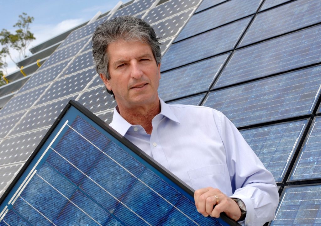
The father of photovoltaic (PV) solar technology: Professor Green
The solar cell was invented when Russel Shoemaker Ohl, a researcher at Bell Labs in the US, noticed in 1940 that a cracked silicon sample produced a current when exposed to light. However, little improvement had been made until the contribution of Martin Green, a young engineering professor working out of the University of New South Wales, Australia.
Born in Brisbane, Queensland, Australia, Green had spent some time in Canada as a researcher before going back to Australia in 1974. A year later he had started a PV solar research group working out of a small laboratory built with unwanted equipment sourced from major American firms.
His first experiments, alongside a single PhD student, involved looking for ways to increase the voltage on early solar cells.
Professor Green, an important pioneer of the PV industry ,
Not long after, Green and his team began to raise their ambitions.. Having boosted the voltage, the next step was building better quality cells. The early efforts broke the world efficiency record in 1983. The team continued to achieve efficiency records in the next 38 years.
In the very early years of the PV industry, the received wisdom had been that a 20 per cent conversion rate marked the hard limit of what was possible from PV solar cells. Green, however, disagreed in a paper published in 1984. A year later, his team built the first cell that pushed past that limit, and in 1989 built the first solar panel capable of running at 20 per cent efficiency.
It was a moment that opened what was possible from the industry, and the new upper limit was set at “25 per cent”—another barrier Green and his team would smash in 2008. In 2015, they built the world’s most efficient solar cell, achieving a 40.6 per cent conversion ion rate using focused light reflected off a mirror.
Enter the sun king
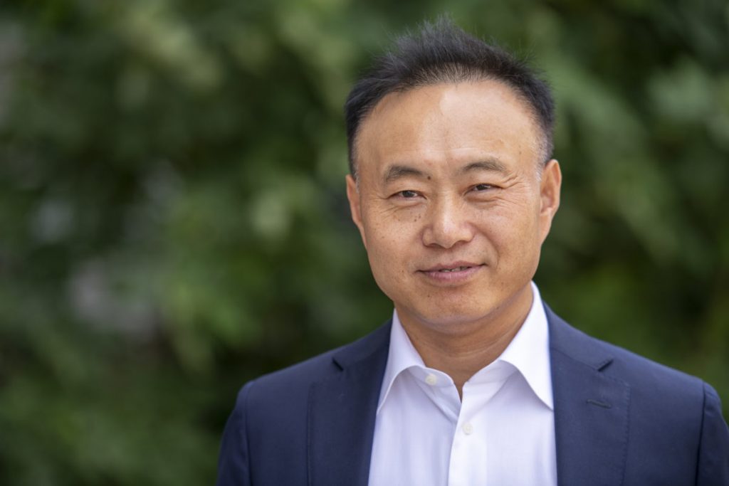
Out of this activity, the Chinse solar industry would be born largely thanks to a ambitious physicist named Zhengrong Shi. Born in 1963, Shi had earned his master’s degree and come to Australu in 1988. He had spotted a flyer advertising a research fellowship and talked to Green into bringing him as a PhD student in 1989. Shi would finish his PhD in just two and half years. He stayed on a as a researcher.
Dr Shi, who kick-started the Chinese PV solar industry
With time, the university was increasingly looking to commercialize its world leading solar cell technology and reached a partnership agreement with t Pacific Power, an Australian power generator in 1995. The Pacific Power invested US$47 million into a new company called Pacific Solar. A factory was set up in the Sydney suburb of Botany and Shi was made the deputy director of research and development.
Shi worked in the company for a few years. In November 2000, he was made an offer. At a dinner held at his home , four officials from the Chinese province of Jiangsu suggested the 37-yaer-ol researcher and Australian citizen return to China and build his own factory there. After some consideration, Shi agreed and ended settling in the small city of Wuxi where he founded SunTech with US46 million in start-up funding from the municipal government.
Shi’s arrival caused a stir in China. The ability to cheaply build conventional solar panels with 17 percent efficiency was far beyond what his competitors were capable off. Shi was quoted; “The first reaction was: that’s the future. Everybody said that’s the future. But they also said it was one step too early. What they meant was that there was no market for it yet. In China, at that time, if you mentioned solar, people thought of solar hot water”.
All that change when Germany passed new laws encouraging the uptake of solar power. Quickly it became clear there was a massive global demand and the world’s manufacturers were struggling to keep up with supply.
Spying an opportunity for investment, a consortium that included Actis Capital and Goldman Sachs came knocking to pitch Shi on taking the company public. When the company listed on the New York Stock Exchange in 2005, it raised US$420 million and made Shi an instant billionaire. A year later he would be worth an estimated US$3 billion and crowned the richest man in China, earning him the moniker “the Sun King”.
As Shi had shown the way, the Chinese PV solar industry began a massive expansion. SunTech alone boosted its production capacity from 60 megawatts (MW) to 500MV, and then 1 gigawatt in 2009. The company grew so fast, its supplies of glass, polysilicon and electronic systems needed to build its panels came under strain, forcing it to invest heavily in local supply chains.
Around 2012 the world market was flooded with solar panels, sending the price plummeting through the floor, leaving SunTech vulnerable. Already under intense financial pressure, disaster struck when an internal investigation found a takeover bid it had launched had been guaranteed by Euro560 million in fake German government bonds. Upon discovering the bonds didn’t exist, Shi was removed as CEO of his company and a year later SunTech would file for bankruptcy protection when it couldn’t repay US$541 million loan that fell due in March 2013.
Chinese manufacturers dominate the PV solar industry
Between 2008 and 2013, China’s fledgling solar panel industry dropped the world’s prices by 80 per cent, a stunning achievement in a fiercely competitive high technology market. Today, the PV solar industry is worth US$100 billion a year.
As a result, China has eclipsed the leadership of the US solar industry, which invented the technology, still holds many of the worlds’ patents and led that industry for more than three decades. Now China dominates nearly all aspects of solar use and manufacturing.
I can now buy Chinese solar flood lights at cheap prices to light my garden at night. Thank you Professor Green and Dr Shi for your pioneering works on the PV solar technology.
References:
Royce Kurmelovs. Insanely cheap energy: how solr power continues to shock the world. The Guardian, April 24th, 2021.
John Fialka. Why China is dominating the solar industry. Scientific American, December 19th, 2016.
Two small companies believe that
they are on the verge of a breakthrough that had eluded scientists for decades
according to Clive Cookson in an article in Financial Times, dated December 29th,
2019.
This fusion breakthrough would
deliver clean and cheap energy by harnessing the nuclear fusion reaction that
powers the sun. The two companies use different approaches to generate the
fusion reaction.
The failure of sustained attempts to develop fusion power since the 1950’s has not deterred investors from backing scientists at Tokamak Energy and First Light Fusion, two private laboratories based in Oxfordshire, England.
Investors have injected £50 million
into Tokamak Energy and £25 million into First Light Fusion. They are seeking
to deliver a working reactor ready for commercialization by 2030.
This would be 10 years earlier than the UK Atomic Energy Authority, which runs the state-funded programme. Back in the 1950’s, the UKAEA built the Zeta fusion reactor, which was hailed at the time as a British technological achievement. It closed in 1968 having failed to produce any useful energy.
The UKAEA is working on a new generation of fusion reactors based on the “tokamak” design that originated in the Soviet Union in the 1050’s. This reaction vessel holds the fuel—a plasma of super-heated deuterium and tritium –in place with powerful magnets while raising its temperature above 100mC so that atomic nuclei fuse and release vast amounts of energy.
The UKAEA is working on the design
for its next-generation Spherical Tokamak for Energy Production reactor, known
as Step, for which the British government has announced £220 million of public
investment.
“The Step reactor will be an
innovative plan for a commercially-driven fusion power station, offering the
realistic prospect of constructing by 2024,” said Ian Chapman, UKAEA chief
executive.
The two private companies have even
more ambitious schedules.
“We are on course for 100mC, the
temperature at which fusion could begin by next March, 2020,“ said David
Kingham, executive vice-chairman of Tokamak Energy. Its target is to generate
fusion power by 2025 and have a commercial plant by 2030.
First Light Fusion, spun out of
Oxford University eight years ago, is
pioneering a different approach. Instead of the reactants within a strong
magnetic field and super-heating them, it aims to achieve the extreme
conditions required to initiate fusion by firing a large number of small copper
projectiles simultaneously at hypersonic speed into a tiny capsule containing
the deuterium and tritium fuel.
First Light Fusion’s pulsed fusion reactor
“While magnetic fusion is like a
furnace that is always on, our projectile fusion is a pulsed process that
transfers energy from each shot into liquid lithium coolant, ” said Nick
Hawker, First Light chief executive.
He said the company expected to demonstrate in early 2020 that the system achieves fusion and aim for “gain”, which is when the reactor generates more energy than is used to spark the reaction, by 2024.
“We understand that government labs
need to be more cautious in their schedules,” said Mr Kingham. “We envisage
having a 150MW device that we can license to people who are good at building
power plants.”
First Light is already working with
the engineering company Mott MacDonald on a commercial reactor design, with the
aim of having a fusion plant powering the grid by the early 2030s. “I am very
supportive of the private fusion companies and UKAEA is committed to working
with them to help develop their technology,” said Mr Chapman. “The promise of
fusion is so huge that there will always be a place for innovation in design.”
Meanwhile, the UKAEA continues to
manage the country’s involvement in big international fusion projects. At
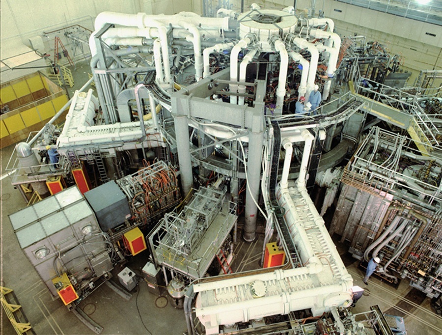
Culham, England, it hosts the Joint
European Torus or JET, the world’s largest and most powerful tokamak reactor and
the focus of the EU’s fusion research programme. JET has been operating since
1983.
A highlight came in 1997 when it was
fuelled with a deuterium-tritium reaction mixture and achieved a world record
for fusion power of 16 megawatts in 1997, though this was less than the energy
put in to heat up the plasma. In recent years, experiments at JET have assisted
the design and construction of ITER, a large-scale fusion machine with a
reaction vessel 10 metres high (compared with 4.3 metres for JET) which is
being built by a global consortium of governments in southern France.
Beset with delays and cost overruns — the current estimate is US$22 billion— ITER is now set to start operating in 2025. The schedule calls for JET to operate at least until 2024, including more runs with deuterium-tritium fuel, though this programme will depend on the UK’s post-Brexit relationship with the EU and Euratom. Although no one knows exactly when commercial fusion power will arrive — and in what form — Mr Chapman expressed total confidence in its eventual arrival. “We will have fusion,” he said, “and Oxfordshire will be closely involved in making it happen.”
Chinese scientists say
they have completed construction of a nuclear fusion reactor that will take
them on the mammoth pursuit of a virtually unlimited source of power.
The machine, based at
the Southwestern Institute of Physics in Chengdu, the capital city of southwest
China’s Sichuan province, will become operational in 2020.
China is among several
states working on projects to achieve nuclear fusion, the atomic reaction that
takes place in the sun and in hydrogen bombs.
The Chinese device
consists of a doughnut-shaped chamber called a tokamak, which is similar to the
EU-funded Joint European Torus in the UK.
The potential prize is
an invaluable contribution to reducing planet-warming emissions. Fusion
reactions release no carbon dioxide. Their fuel, derived from water, is
abundant.
Experiments in China’s
reactor will provide a dress rehearsal for work on ITER.
The Chinese are one of
seven main partners – alongside the EU, Japan, Russia, the US, India and South
Korea – in ITER, the world’s most expensive international science project, at
£15.5 billion.
All partners have
agreed to contribute pieces of the reactor, with the central ITER organisation
responsible for coordinating construction. The EU owns 45 per cent of the
project and the other partners nine per cent each.
ITER promises to
produce net fusion power sometime after 2035.
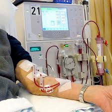
People with kidney failure could soon be spared regular trips to
hospital thanks to a new dialysis machine the size of a microwave.
My late father used to visit a government dialysis centre twice a week,
for almost 10 years. Fortunately, we had a friend who ferried him to the dialysis
centre, which was about 10 km from our house. Some kidney patients are less
fortunate who had to travel a distance to receive a dialysis treatment.
A British company, Quanta, had announced that it had has raised £38m from investors to launch a much smaller than traditional dialysis machines, called SC+. Currently only 5 per cent of UK kidney patients, some 1,500 people, are treated at home. Quanta, based in Warwickshire, United Kingdom, said patients could be taught how to use the SC+ either at home or at a self-service clinic.
Quanta’s compact dialysis machine
John Milad, head of Quanta, said the device would allow dialysis
patients to take “greater control of their lives”. In the future, dialysis
could be as easy as visiting a “cash machine”.
“We believe there should be tens of thousands of them,” he added.
Approximately 3.5m people around the world require dialysis treatment.
Quanta was spun out of British engineering giant IMI in 2008, and was
created after the technology used to mix soft drinks in bars was applied to
blood dialysis. It now plans to ask for permission to launch the new compact dialysis
machine in the US this year.
The cash injection came from several investors, including a private
Swiss family office, Wellington Partners and Seroba Life Sciences.
Lifestyle choices, modern diet and increased life expectancy are
all negatively impacting renal health across the globe and End Stage Renal
Disease (ESRD) affects millions of patients worldwide. Haemodialysis is a
lifesaving treatment delivered to an estimated 3 million people globally, with
this figure expected to double in the next decade.
At present, haemodialysis is
primarily provided by specialist clinics and centres. The rigid clinic
scheduling means that the patient is not in control of when they can dialyse.
It is clinically proven that more regular dialysis improves outcomes and quality
of life for the patient, and a number of studies have shown that 30-40% of
patients would be capable of performing self-care dialysis.
Issues of patient benefit, cost and clinic capacity are driving the growth of home and self-care modalities of haemodialysis. A major factor limiting the growth of self-care and home haemodialysis is the lack of convenient, compact and easy-to-use dialysis systems. Quanta addresses these issues and puts the focus on the patient, allowing them to take greater control of their treatment.